
From Tea Gardens to Microchips: Inside Assam’s ₹27,000-Crore Semiconductor Revolution
Krosstale Media Desk
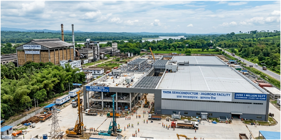
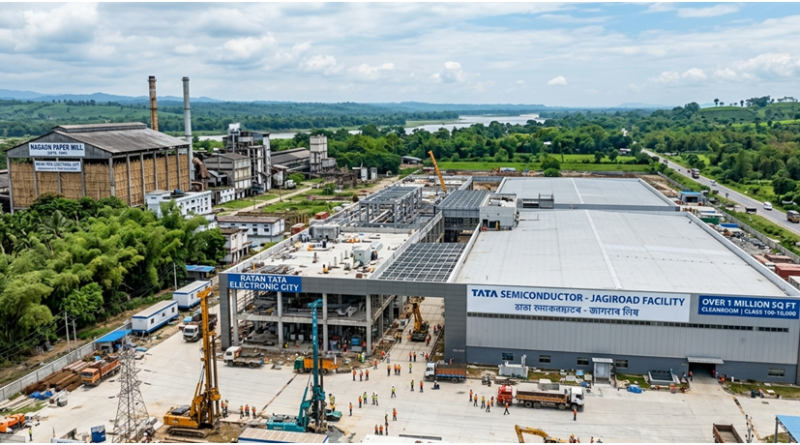
The state of Assam, historically identified with its vast tea estates, agrarian base, and natural resource extraction industries, is undergoing an unprecedented structural transition towards advanced high-technology manufacturing. At the core of this transformation is the INR 27,000-crore (approximately $3.6 billion) greenfield semiconductor packaging and assembly facility under development in Jagiroad, located within the Morigaon district.
Underwritten by Tata Semiconductor Assembly and Test Private Limited (TSAT), a subsidiary of the Tata Group, this development marks the establishment of India’s first indigenous greenfield Outsourced Semiconductor Assembly and Test (OSAT) plant.
The plant represents a major triumph for the India Semiconductor Mission (ISM) and signals a geographical diversification of the country’s technology footprint, bringing the historically under-industrialised Northeast region into the global microelectronics supply chain. With construction progressing rapidly and initial cleanroom qualification underway, the facility is poised to commence commercial production within the current fiscal year.
The Historical Rebirth of the Jagiroad Site
The selection of the Jagiroad site carries profound historical, industrial, and social significance. The facility is being constructed on the 592-acre property of the defunct Nagaon Paper Mill, which was originally established in 1985 under the state-owned Hindustan Paper Corporation Limited. As a historical landmark, the Nagaon Paper Mill was once celebrated as the first industrial facility in the world to successfully produce Kraft pulp in a Kamyr Continuous Digester utilising 100% bamboo raw material.
Despite operating beyond its installed capacity and remaining highly profitable for decades, severe financial distress led to the abrupt halting of its operations in October 2017. The subsequent liquidation process under the National Company Law Tribunal left thousands of workers without employment or salaries, resulting in a prolonged socio-economic crisis.
In March 2022, the Government of Assam intervened by purchasing the assets of both the Nagaon Paper Mill and the Cachar Paper Mill for INR 375 crore, utilising funds from a cabinet-approved package of INR 700 crore designed to clear outstanding operational and employee liabilities. By transitioning this defunct industrial site into the “Ratan Tata Electronic City,” the state government has successfully repurposed a legacy brownfield site for the clean, high-value-added semiconductor manufacturing sector.
The site is strategically positioned roughly 55 kilometres east of Guwahati and 76 kilometres from the Lokpriya Gopinath Bordoloi International Airport, with robust links to National Highway 37, rail freight networks, and the Brahmaputra River. This multimodal logistics infrastructure ensures that heavy manufacturing equipment can be imported, and finished microchips can be exported, with minimal transit friction.
Physical Infrastructure and Site Engineering
Converting a legacy paper mill into an advanced semiconductor cleanroom requires a complete overhaul of the physical and environmental systems. Semiconductor back-end packaging processes require an environment entirely free of airborne particulates, static charge, and micro-vibrations, all of which can compromise the integrity of sub-micron interconnects. Consequently, Tata Consulting Engineers (TCE) is utilising integrated Building Information Modelling (BIM) 3D design practices to manage the engineering complexity of the site.
The site’s physical design and construction parameters are structured to support continuous high-volume operations:
| Infrastructure Category | Technical Specification or Requirement | Operational and Engineering Purpose |
| Campus Size | 171 acres (within the broader 592-acre site). | Houses the high-volume packaging plant, sub-stations, and logistics hubs. |
| Cleanroom Space | Over 1 million square feet (>1 Mn ft²). | Provides a Class 100 to Class 10,000 dust-free environment for wafer handling and wire bonding. |
| Substructural Foundation | Deep piling with specialized, vibration-damped concrete flooring. | Eliminates low-frequency ambient vibrations from nearby highways and railways that disrupt automated tool precision. |
| Environmental Controls | Dedicated HVAC systems with multi-stage HEPA filtration. | Maintains strict temperature, relative humidity, and electrostatic discharge (ESD) standards. |
| Power Infrastructure | High-voltage dual-source grid connection backed by on-site solar power. | Ensures uninterrupted power quality; cleanrooms cannot tolerate even millisecond-scale power drops. |
| Water Management | Industrial-scale water treatment with advanced recycling and conservation protocols. | Supplies ultra-pure water (UPW) for wafer dicing and cleaning while adhering to strict ESG principles. |
Back-End Manufacturing Technologies and Phased Ramp-Up
In the semiconductor manufacturing process, back-end packaging constitutes the final value-addition step. Silicon wafers fabricated at front-end foundries are sent to OSAT plants, where they are diced into individual dies, interconnected to a substrate, encapsulated in protective packaging, and rigorously tested. The packaging provides physical protection from mechanical shock and moisture, manages thermal dissipation, and establishes electrical pathways between the silicon die and the printed circuit board.
The Jagiroad plant will initially employ three core packaging and interconnection technologies:
- Wire Bond: This traditional yet reliable method uses fine wires of gold, copper, or aluminium to connect the die to the leadframe. It is ideal for cost-sensitive, lower-pin-count applications such as power management systems and automotive sensors.
- Flip Chip: In this high-density method, solder bumps are deposited on the top surface of the die, which is then flipped and bonded directly to the substrate. This shortens signal paths, reduces parasitic inductance, and enhances thermal management, making it suitable for high-speed processors and RF modules.
- Integrated Systems Packaging (ISP): This advanced approach integrates multiple heterogeneous dies—such as processors, high-bandwidth memory (HBM), and passive components—into a single high-performance package, supporting the industry’s transition towards software-defined platforms.
Rather than attempting an immediate full-capacity launch of 48 million chips per day, Tata Electronics is implementing a phased commissioning model, which is the standard protocol for qualifying cleanroom yields, verifying logistics, and calibrating high-precision assembly tools. To accelerate the initial learning curve, the company is relocating an entire operational product line, complete with its engineering team and process recipes, from its early commercial facility in Vemgal, Karnataka, to Jagiroad. This transfer allows TSAT to bypass early qualification hurdles and establish high-yield manufacturing baselines in Assam.
Yield stability is particularly critical for the plant’s automotive product lines. Standard automotive-grade semiconductors must comply with the AEC-Q100 reliability standard, requiring components to operate reliably across extreme temperature ranges (from under-hood engine heat to freezing winter environments) while withstanding sustained physical vibration. Because a single microscopic defect in the encapsulation or interconnection can render a complex automotive system inoperable, the slow scaling of cleanrooms acts as a risk-mitigation strategy before high-volume commercial shipments begin.
Global Strategic Partnerships and Anchor Customers
The long-term commercial viability of any greenfield OSAT plant is determined by its integration with global technology leaders and its ability to secure anchor customers. The Jagiroad facility has successfully secured high-profile global agreements that position it as a critical node in the global semiconductor value chain.
A milestone partnership was established in early 2026, when Qualcomm Technologies announced that it would utilise the Jagiroad facility to manufacture its Qualcomm Automotive Modules in India. This agreement integrates the facility into Qualcomm’s global module manufacturing network. The modules will integrate Qualcomm’s Snapdragon Digital Chassis system-on-chips (SoCs) with supporting power management, RF, and passive components into a single, production-ready system. This system-in-package approach reduces design complexity for automakers, allowing them to rapidly deploy advanced digital cockpits, real-time connectivity, ADAS, and intelligent infotainment platforms.
Furthermore, Tata Electronics has secured additional global supply agreements to build a robust commercial ecosystem:
| Partner Organisation | Nature of Agreement | Strategic and Technological Implication |
| Qualcomm Technologies | Manufacturing partner for Snapdragon-based Automotive Modules. | Establishes the facility as a tier-one supplier for global and domestic automotive OEMs. |
| Tesla | Strategic semiconductor procurement agreement (signed April 2024). | Secures a high-volume global electric vehicle client, validating the plant’s AEC-Q100 automotive qualification. |
| Analog Devices (ADI) | Strategic alliance for joint technology development (forged September 2024). | Enhances technical capabilities in analog-to-digital conversion and power management IC packaging. |
| ASML | Strategic technology and equipment partnership. | Secures access to cutting-edge photolithography support and specialized machinery maintenance. |
These collaborations ensure that the facility serves as a trusted partner for both global technology giants and domestic electronics companies seeking to build resilient supply chains. Ultimately, future consumer electronics, telecommunications infrastructure, and vehicles driven worldwide will be powered by chips assembled and packaged in Jagiroad.
Policy Alignment and Geopolitical Context
The establishment of the Jagiroad plant highlights a successful coordination between national industrial ambitions and regional policy frameworks. At the national level, the India Semiconductor Mission (ISM) provides capital support, covering up to 50% of the total project cost on a pari-passu basis for approved semiconductor packaging and fabrication facilities. This represents a strategic shift from the original ISM 1.0, which focused primarily on capacity building, to ISM 2.0, which places greater emphasis on equipment, specialized chemicals, materials, IP design, and the development of robust localized supply chains.
The Government of Assam has complemented these national incentives through a three-policy framework, integrating:
- Assam’s Electronics Policy & Component Manufacturing Policy: Providing regional capital subsidies, power tariffs, and tax exemptions tailored for high-tech investments.
- The Central Government’s UNNATI Scheme: A dedicated fiscal program designed to incentivize industrial development and capital investment in Northeast India.
- Asian Development Bank (ADB) Infrastructure Funding: Negotiations for dedicated loans to meet the transport and utility needs of the “Ratan Tata Electronic City”.
This policy framework contrasts with the semiconductor strategies of other nations. For instance, while China’s semiconductor policy is largely inward-looking—driven by massive state funding aimed at bypassing Western export controls and replacing American components—India’s approach is fundamentally collaborative and outward-looking. By leveraging agreements with global technology leaders (such as Qualcomm and Tesla), India is positioning itself as a reliable, alternative manufacturing hub in the global technology supply chain.
Additionally, the facility’s design is heavily aligned with modern Environmental, Social, and Governance (ESG) standards. This commitment is demonstrated through the integration of solar power arrays, high-efficiency manufacturing processes, and advanced water recycling systems, satisfying the sustainability requirements of international tech firms.
Demographic Shifts and Local Human Capital Development
The socio-economic impact of the TSAT plant extends far beyond direct hardware assembly. Historically, the northeastern states of India have suffered from a lack of high-technology employment opportunities, forcing thousands of engineering and technical graduates to migrate to southern technology hubs in search of employment—a domestic brain drain.
The establishment of the Jagiroad plant is reversing this trend. Tata Electronics is actively recruiting skilled Assamese professionals from around the country and abroad, importing global industrial expertise to build a local technology workforce.
To ensure a steady talent pipeline, State Industries and Commerce Minister Bimal Bora has detailed a structured recruitment and training program in partnership with leading educational institutions. The plant’s direct workforce is projected to reach approximately 15,700 people, broken down across the following demographics:
TSAT Jagiroad Direct Workforce Demographics
- Operators & Technicians: 9,000
- Service Staff: 2,200
- Engineers: 1,700
- Quality & Store Staff: 1,600
- Supervisors: 1,000
- Managers & Leadership: 600
This workforce requirement is supported by targeted academic and vocational initiatives:
- Assam Skill University: Backed by an INR 1,000-crore loan from the Asian Development Bank, classes are starting under a curriculum specifically tailored to semiconductor packaging, cleanroom protocols, and automated manufacturing.
- National Institute of Electronics and Information Technology (NIELIT) & Tata MoU: Signed in January 2025, this agreement creates a co-located skill development centre directly on the Jagiroad campus to provide hands-on vocational training.
- IIT Guwahati Integration: Developing specialised courses and academic programs in VLSI design, semiconductor manufacturing, and advanced testing. This curriculum is designed to produce high-level R&D talent alongside the state’s broader target of skilling 5,000 individuals annually in advanced semiconductor systems.
- Grassroots Community Engagement: Organisations such as the North East India Scientific and Entrepreneurial Diaspora (NEISEDS) have initiated outreach programs at institutions like Jagiroad College. Under the direction of experts such as Sanjeev Hazarika, these workshops introduce local students to career pathways in the design and manufacturing verticals, ensuring that rural youth are prepared for technical opportunities.
The high demand for these roles and the rapid transition of the local economy have also created new regulatory and security challenges. The intense local competition for employment was highlighted in late 2025 and early 2026 when state police uncovered a sophisticated recruitment scam. A criminal ring led by Tarikul Ahmed, who falsely posed as a senior engineer at the facility, duped hundreds of local youth under the guise of offering guaranteed jobs at the Tata plant.
The subsequent police investigation led to multiple arrests, including a college lecturer, and the freezing of bank accounts containing over INR 25 lakh. While a security concern, this incident underscores the high local expectations, the economic value associated with the facility, and the urgent need for transparent, institutional recruitment pathways.
Future Regional Transformation and Industrial Clustering
During the Advantage Assam 2.0 Investment and Infrastructure Summit, Tata Sons Chairman N. Chandrasekaran announced that the initial OSAT facility is only the first phase of a broader commitment. The Tata Group plans to invest an additional INR 27,000 crore over the next five years to establish a complementary electronics, urban infrastructure, and mobile technology manufacturing cluster in Assam, with the goal of creating an additional 30,000 high-technology jobs.
This secondary expansion is already attracting a support network of ancillary suppliers. During the same summit, 14 bilateral Memorandums of Understanding (MoUs) were signed with global semiconductor supply chain companies, including DISCO Corporation and Resonac Holdings of Japan, alongside United States-based suppliers Heraeus Industries and ECA Advanced Solutions. These companies are evaluating plans to co-locate material testing, precision tooling, calibration services, and chemical supply hubs within the Jagiroad cluster.
Additionally, global logistics and freight providers such as DHL, Container Corporation of India (CONCOR), and Nippon Express have expressed interest in establishing dedicated production and transport hubs near the facility. This clustering of transport networks and advanced engineering services ensures that Jagiroad will transform from a singular factory site into a self-sustaining industrial ecosystem.
Conclusion
The economic transition from the defunct paper mill to a greenfield semiconductor facility is a notable success story for regional development. By combining central capital subsidies, state-level policy support, and partnerships with global brands like Qualcomm and Tesla, Assam is establishing a resilient, high-technology economy. As commercial production begins, this microchip revolution will write a new chapter in the industrial history of Northeast India.